Digilent Atlys
Before loading the gateware you need to set the jumpers correctly and connect the cables correctly.
FIXME: Put something here about the Atlys.
As the HDMI2USB firmware manipulates the EDID information the following jumpers must be removed;
JP2/SDA (which connects the EDID lines from J1/HDMI IN to JA/HDMI OUT).
JP6 and JP7 (which connects the EDID lines from J3/HDMI IN to J2/HDMI OUT).
-
Plug board in using
PROGport & switch on. If using a VM, ensure the device is passed through. -
The other UART port is for the controlling the firmware. Recommend plugging this in too so you can use/test the device.
The Digilent Atlys board is the primary development platform for the HDMI2USB project.
Step 0 - Buy Atlys Board from Digilent
Step 1 - Customizing the board - Customizing the board is not needed.
Step 2 - Loading Firmware
Step 3 - Testing and Troubleshooting
Step 4 - Set up the Development Environment This step is only required if you need to "unbrick" a Digilent Atlys board which has been permanently programmed as a HDMI2USB device and has failed.
First find JP9 next to USB PROG connector.
See image 
Turn over the board and look at the bottom of JP9
See image 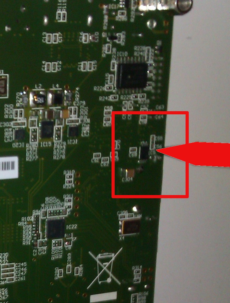
You need to break a track joining the two pads for JP9.

Solder a jumper onto the pads.
After following modifications use the listed process below;
- Remove the JP9 jumper.
- Turn on the power, the device should appear as an unconfigured Cypress chip
- Program the Cypress chip EEPROM loading code.
- Download new firmware into the EEPROM.
- Put the JP9 jumper back on.
- Power cycle the board.
- Please see https://github.com/timvideos/HDMI2USB-misoc-firmware repo.
FIXME: Write instructions for the correct jumper configuration of the board.
As the HDMI2USB firmware manipulates the EDID information the following jumpers must be removed;
- JP2 (which connects the EDID lines from J1/HDMI IN to JA/HDMI OUT).
- JP6 and JP7 (which connects the EDID lines from J3/HDMI IN to J2/HDMI OUT).
This is described in the Atlys™ Board Reference Manual on "Video Input and Output (HDMI Ports)" (page 13).
If you wish to program the Digilent Atlys outside of the LiteX Build Environment directly you can use;
To use this method you must have the Adept 2.XX.XX Utilities installed and Adept 2.XX.XX Runtime installed.
- Step 1 - Plug the power from your power pack into the POWER port.
- Step 2 - Plug the micro-USB cable from your computer into the PROG port.
- Step 3 - Run
djtgcfg enum, output should be as follows;
$ djtgcfg enum
No devices found
$- Step 4 - Toggle the POWER switch to the ON position
- Step 5 - Run
djtgcfg enum, output should be as follows; If it doesn't, see the Troubleshooting Digilent Adept tools section
$ djtgcfg enum
Found 1 device(s)

Device: Atlys
    Product Name:   Atlys
    User Name:      Atlys
    Serial Number:  210178440327
$- Step 6 - Run
djtgcfg init -d Atlys, output should be as follows; If it doesn't, see the Troubleshooting Digilent Adept tools section
$ djtgcfg init -d Atlys
Initializing scan chain...
Found Device ID: 44008093

Found 1 device(s):
    Device 0: XC6SLX45
$- Step 7 - Run
djtgcfg prog -d Atlys -i 0 -f hdmi2usb.bit, output should be as follows; If it doesn't, see the Troubleshooting Digilent Adept tools section
$ djtgcfg prog -d Atlys -i 0 -f hdmi2usb.bit
Programming device. Do not touch your board. This may take a few minutes...
Programming succeeded.
$- Step 8 - The DONE light near the red RESET button should light up.
The Xilinx IMPACT tool is useful if you are developing code in Xilinx ISE, so you can do one click download in the Xilinx Design tools.
IMPACT must be installed from the Xilinx Design Tools suite.
FIXME: Add content
To avoid having to use the Impact GUI, the following script can be used https://gist.github.com/shenki/5387626
impact -batch download.cmd
Once Stage 1 has been loaded onto the Atlys board, the HDMI matrix will be initialized.
The HDMI output ports should be showing the following graphic:

If you plug a device into the HDMI input ports, it should successfully detect a 1024x768 screen input. You should be able to switch to it via the buttons. See Digilent Atlys Board: Switches, Buttons and Status LEDs page for more information.
Once you complete Stage 2 you be unable to go back to Stage 1 without a power cycle.
You must either use;
- The fxload
or
- The fx2loader
In both cases, you will need the hdmi2usb.hex file for this stage. Prebuilt firmware blob can be found in the HDMI2USB-firmware-prebuilt repository.
WARNING: The version of fxload that comes with Ubuntu/Debian is too old
You can download fxload from https://github.com/pbatard/fxload or you can use a prebuilt version found at the same location as the prebuild hdmi2usb firmware.
- Step 1 - Check your
fxloadbinary is new enough;
Too old
$ fxload -V
Jun  3 2010 (development)
$
Okay
$ ./fxload -V
Mar 12 2013 (development)
$- Step 2 - Load the Cypress chip with the firmware using
./fxload -vvv -t fx2 -D 1443:0007 -I hdmi2usb.hex. This command will appear to return instantly!
You should also be able to use http://www.makestuff.eu/wordpress/software/fx2tools/
./fx2loader --vidpid=1443:0007 hdmi2usb.hex ram
- Step 1 - Unplug the USB micro-cable connected to PROG. DO NOT DISCONNECT THE POWER
- Step 2 - Plug the USB micro-cable back into the PROG port.
- Step 3 - Check your kernel logs via
dmesgto see if the device is found. It should look something like;
$ dmesg
....
[150303.829773] usb 2-1.1: config 1 interface 2 altsetting 0 endpoint 0x81 has an invalid bInterval 17, changing to 8
[150303.830657] usb 2-1.1: New USB device found, idVendor=fb9a, idProduct=fb9a
[150303.830668] usb 2-1.1: New USB device strings: Mfr=2, Product=1, SerialNumber=1
[150303.830674] usb 2-1.1: Product: HDMI2USB
[150303.830678] usb 2-1.1: Manufacturer: JANI
[150303.830683] usb 2-1.1: SerialNumber: HDMI2USB
[150303.832191] uvcvideo: Found UVC 1.00 device HDMI2USB (fb9a:fb9a)
[150303.832561] uvcvideo: UVC non compliance - GET_DEF(PROBE) not supported. Enabling workaround.
[150303.833719] cdc_acm 2-1.1:1.2: This device cannot do calls on its own. It is not a modem.
[150303.833885] cdc_acm 2-1.1:1.2: ttyACM0: USB ACM device- Step 4 - Use the device as required.
-
Please see https://github.com/timvideos/HDMI2USB-misoc-firmware repo.
This information is copied from the Status LEDs, Push buttons and Jumpers section in the "HDMI2USB - Developers Guide" document. Make sure they are kept in sync!
| Button | Description |
|---|---|
| BTNU (N4) | Selects HDMI 0 as output. |
| BTNL (P4) | Selects HDMI 1 as output. |
| BTNR (F6) | ??? |
| BTND (P3) | Selects test pattern as output. |
| BTNC (F5) | If pressed emulates display connection to read edid structure. |
| SWITCH | DESCRIPTION |
|---|---|
| SW 0 | Turns on/off heart beat pixels |
- Resolution mode - 720p (HDMI mode) or 1024x768 (DVI mode)
- UVC output mode - RAW or MJPEG
| LED | Description |
|---|---|
| LED0 | Indicates HDMI 0 input is connected. |
| LED1 | Indicates HDMI 1 input is connected. |
| LED2 | If on then UVC is MJPEG if off then output is RAW. |
| LED3 | Flab B (Full Flag) of cypress USB device. |
| LED4 | Flab C (Empty Flag) of cypress USB device. |
| LED5 | SLWR signal to cypress USB device. |
| LED7:6 | Combination of LED7 and 6 tells which input source is selected as output to HDMI matrix and USB. |
- LED0 should be on if a HDMI source is connected to HDMI port 0.
- LED1 should be on if a HDMI source is connected to HDMI port 1.
- LED2 - ???
- LED3 should remain off at all times when USB is capturing.
- LED4 should be DIM when USB is capturing.
- LED5 - ????
| LED7, LED6 | Selected Input |
|---|---|
| Off, Off | HDMI 0 |
| Off, On | HDMI 1 |
| On, Off | Reserved (for VGA extension board) |
| On, On | Test pattern |
The important parts of the Digilent Atlys boards are;
-
PGOOD LED- Green LED right under the power switch. -
HDMI Output 0- Labelled J2, found just right of the power switch and left of the audio jacks. -
HDMI In 0- Labelled J3, found between the audio and Ethernet port -
JP8- Found next to the HDMI In 0 -
JP6 & JP7- Found just below JP8 next to each other. They are also labelled SCL and SDA, but the labels are quite hard to read.
-
JP12- Found next to the VHDCI connector -
DONE Led- Found between the RESET switch and the VHDCI connector
-
HDMI Output 1- A small HDMI-D connector on the underside of the PCB in the lower left corner. -
JP3- Also labelled with 5V0 found next to the PMOD header. -
JP2- This header is suppose to be labelled JP2 but is not. It is only labeled SCL and SDA.
-
JP5- Next to that -
HDMI In 1- Labeled J1, found under the USB UART bridge -
JP4- Roughly betweenHDMI In 1and theUART Port -
UART Port- A micro USB Port labelled UART -
JP11- Found just below the full size USB port -
JP9- Between the PROG Micro USB Port and the full size USB port -
PROG Port- A micro USB Port labelled PROG
-
PGOOD LED- This LED must be lit green for anything to work. If it does not light up green then your Atlys board has probably been damaged. -
JP12must have a jumper connecting to either the 3V3 or 2V5 side. If no jumper is connected, the FPGA will not boot. From the Digilent Atlys manual;
Always keep JP12 loaded (either on 3.3V or 2.5V). If JP12 is not loaded, bank 2 of the FPGA is not supplied, and neither are the pull-ups for CCLK, DONE, PROGRAM_B and INIT_B. The FPGA is held in the Reset state, so it is not seen in the JTAG chain, neither can be programmed from the serial FLASH.
-
JP11is used to disable the FPGA from loading the configuration from the onboard SPI flash. This header may not be populated on your board. During normal operation this should not have a jumper on it. This jumper is only needed when loading the HDMI2USB firmware onto the board permanently for the first time. From the Digilent Atlys manual;
An on-board mode jumper (JP11) selects between JTAG/USB and ROM programming modes. If JP11 is not loaded, the FPGA will automatically configure itself from the ROM. If JP11 is loaded, the FPGA will remain idle after power-on until configured from the JTAG or Serial programming port.
-
USB PROGneeds to be connected to the capture computer. It is used for programming the FPGA and for getting the Webcam adata. -
USB UARTneeds to be connected to the capture computer. It is used for controlling the firmware via the serial control.
-
HDMI Out 1andHDMI In 1can not be used at the same time reliably (due to the EDID lines being connected). Only use one or the other unless you really understand what you are doing. -
HDMI Out 1is an unamplified output. Use a very short cable, like 30cm short. -
The Atlys board doesn't have control over the hot plug signal meaning it is unable to reset the HDMI port. This means after a config change you will have to unplug and replug the HDMI Inputs or otherwise force a config refresh.
Make sure the jumpers in the Notes section above are set. Then you need the following configuration;
-
JP4must be connected (connects 5Vs toHDMI In 0). -
JP8must be connected (connects 5Vs toHDMI In 1). -
JP3must be disconnected (removes 5Vs toHDMI Out 1). -
JP6 & JP7must be disconnected (meansHDMI In 0andHDMI Out 0EDID operate independently. -
JP2must be connected (connects EDID toHDMI In 1andHDMI Out 1).- Care must be taken to put the jumpers on JP2 in the right direction. They should be XXXX not XXXX.

USB Micro PROG --> Capture Computer

Presenters Laptop --> HDMI Input 0
Capture Computer  --> HDMI Input 1

HDMI Output 0 --> Projector
HDMI Output 1 --> Confidence Monitor

| J1: IN | J2: Out | J3: IN | JA: BiDi | ||
|---|---|---|---|---|---|
| Type | HDMI Type A | HDMI Type A | HDMI Type A | - | HDMI Micro D |
| Location | - | ||||
| Pin / Signal | FPGA Pin | FPGA Pin | FPGA Pin | Pin/Signal | FPGA Pin |
| 1: D2+ | B12 | B8 | J16 | 1: HPD | JP3 |
| 2: D2_S | GND | GND | GND | 2: RES | VCCB2 |
| 3: D2- | A12 | A8 | J18 | 3: D2+ | N5 |
| 4: D1+ | B11 | C7 | L17 | 4: D2_S | GND |
| 5: D1_S | GND | GND | GND | 5: D2- | P6 |
| 6: D1- | A11 | A7 | L18 | 6: D1+ | T4 |
| 7: D0+ | G9 | D8 | K17 | 7: D1_S | GND |
| 8: D0_S | GND | GND | GND | 8: D1- | V4 |
| 9: D0- | F9 | C8 | K18 | 9: D0+ | R3 |
| 10: Clk+ | D11 | B6 | H17 | 10: D0_S | GND |
| 11: Clk_S | GND | GND | GND | 11: D0- | T3 |
| 12: Clk- | C11 | A6 | H18 | 12: Clk+ | T9 |
| 13: CEC | NC | 0K to Gnd | NC | 13: Clk_S | GND |
| 14: RES | NC | NC | NC | 14: Clk- | V9 |
| 15: SCL | C13 | D9 | M16 | 15: CEC | VCCB2 |
| 16: SDA | A13 | C9 | M18 | 16: Gnd | GND |
| 17: Gnd | GND | GND | GND | 17: SCL | C13[2] |
| 18: 5V | JP4[1] | 5V | JP8[1] | 18: SCA | A13[2] |
| 19: HPD | 1K to 5V | NC | 1K to 5V | 19: 5V | JP3 |
- [1]: jumper can disconnect Vdd
- [2]: shared with J1 I2C signals via jumper JP2
For HDMI Input (HDMI Sink)
-
HPD should be pulled high.
-
5V pin should disconnected.
-
There is some indication that crappy computers use the 5V pin for detection rather than HPD. Hence maybe we need to connect the 5V?
For HDMI Output (HDMI Source)
- HPD should be pulled low.
- 5V pin should be connected. The Atlys board includes a USB-UART bridge(Exar XR21V1410) which allows serial communication between FPGA and Host. The driver provided by Exar is outdated and does not work on newer Linux Kernel. Driver compatible with latest linux kernel can be found here.
Download driver
git clone https://github.com/shenki/exar-uart-driver.gitTo install first remove old driver. Disconnect the USB-UART if it is already connected.
sudo rmmod cdc-acm
sudo rmmod vizzini
sudo modprobe -r usbserial
Install Drivers
cd exar-uart-driver
sudo modprobe usbserial
sudo insmod ./vizzini.ko
Connect the UART-USB bridge. The device should enumerated as dev/ttyUSBx.
To check whether the driver is successfully installed:
dmesg | grep -i ttyOuput
......
[10118.569307] vizzini 3-2.3:1.0: ttyUSB0: XR21v14x usb uart device
.....
``` * Please see https://github.com/timvideos/HDMI2USB-misoc-firmware/blob/master/scripts/README.md#prerequisite

<br>
<br>
<br>
<br>
<br>
<br>
<br>
<br>
<br>
<br>
<br>
<br>
<br>
<br>
<br>
<br>
<br>
<br>
<br>
<br>
<br>
<br>
<br>
<br>
<br>
<br>
<br>
<br>
<br>
<br>
<br>
<br>
<br>
<br>
<br>
<br>
<br>
<br>
<br>
<br>

<hr>
<hr>
<hr>

# Setting up Adept Tools

These instructions are for setting up Adept tools for usage with Digilent Atlys board and the Xilinx ISE tools.

Download Xilinx ISE. The current version is 14.7 and released on the Oct 23, 2013.
http://www.xilinx.com/support/download/index.html/content/xilinx/en/downloadNav/design-tools.html "Full Installer for Linux (TAR/GZIP - 6.09 GB)" MD5 SUM Value: e8065b2ffb411bb74ae32efa475f9817
These instructions are based off of the instructions found at http://lighttomorrow.wordpress.com/2011/12/18/how-to-install-digilent-cable-driver-for-xilinx-design-suite-on-ubuntu-11-10/ and http://wiki.gentoo.org/wiki/Xilinx_USB_JTAG_Programmers#Digilent_Xilinx_USB_JTAG_cable but updated to use the latest Adept information.
digilent.adept.runtime_2.13.1-x86_64 digilent.adept.utilities_2.1.1-x86_64 libCseDigilent_2.5.2-x86_64
```bash
# This assumes that ISE was installed to /opt/Xilinx/
tar -zxvf libCseDigilent_2.5.2-x86_64.tar.gz
cd libCseDigilent_2.5.2-x86_64/ISE14x
sudo mkdir -p /opt/Xilinx/14.4/ISE_DS/ISE/lib/lin64/plugins/Digilent/libCseDigilent/
sudo cp plugin/* /opt/Xilinx/14.4/ISE_DS/ISE/lib/lin64/plugins/Digilent/libCseDigilent/
Running IMPACT
. /opt/Xilinx/14.4/ISE_DS/settings64.sh
impact
If you get errors like WARNING:iMPACT - Module windrvr6 is not loaded. Please reinstall the cable drivers. See Answer Record 22648. or WARNING:iMPACT:923 - Can not find cable, check cable setup ! then the Digilent Adept plugin is not been successfully found. Try following the install instructions again.
You should get an image which looks like this;
INFO:iMPACT - Current time: 20/04/14 3:03 PM
// *** BATCH CMD : ReadIdcode -p 1
Maximum TCK operating frequency for this device chain: 0.
Validating chain...
Boundary-scan chain validated successfully.
'1': IDCODE is '01000100000000001000000010010011'
'1': IDCODE is '44008093' (in hex).
'1': : Manufacturer's ID = Xilinx xc6slx45, Version : 4
INFO:iMPACT - Current time: 20/04/14 3:05 PM
// *** BATCH CMD : ReadUsercode -p 1
Maximum TCK operating frequency for this device chain: 0.
Validating chain...
Boundary-scan chain validated successfully.
'1': Usercode is 'ffffffff'
INFO:iMPACT - Current time: 20/04/14 3:05 PM
// *** BATCH CMD : ReadStatusRegister -p 1
Maximum TCK operating frequency for this device chain: 0.
Validating chain...
Boundary-scan chain validated successfully.
'1': Reading bootsts register contents...
[0] VALID_0 - ERROR OR END OF STARTUP (EOS) DETECTED                       :         1
[1] FALLBACK_0 - FALLBACK RECONFIGURATION ATTEMPT DETECTED                 :         0
[2] RESERVED                                                               :         0
[3] WTO_ERROR_0 - WATCHDOG TIME OUT ERROR                                  :         0
[4] ID_ERROR_0 - FPGA DEVICE IDCODE ERROR                                  :         0
[5] CRC_ERROR_0 - CYCLIC REDUNDANCY CHECK (CRC) ERROR                      :         0
[6] VALID_1 - ERROR OR END OF STARTUP (EOS) DETECTED                       :         0
[7] FALLBACK_1 - FALLBACK RECONFIGURATION ATTEMPT DETECTED                 :         0
[8] RESERVED                                                               :         0
[9] WTO_ERROR_1 - WATCHDOG TIME OUT ERROR                                  :         0
[10] ID_ERROR_1 - FPGA DEVICE IDCODE ERROR                                 :         0
[11] CRC_ERROR_1 - CYCLIC REDUNDANCY CHECK (CRC) ERROR                     :         0
[12] STRIKE CNT - STRIKE COUNT FOR FALLBACK ATTEMPTS                       :         0
[13] STRIKE_CNT - STRIKE COUNT FOR FALLBACK ATTEMPTS                       :         0
[14] STRIKE_CNT - STRIKE COUNT FOR FALLBACK ATTEMPTS                       :         0
[15] STRIKE_CNT - STRIKE COUNT FOR FALLBACK ATTEMPTS                       :         0
'1': Reading status register contents...
[0] CRC ERROR                                                              :         0
[1] IDCODE ERROR                                                           :         0
[2] DCM LOCK STATUS                                                        :         1
[3] GTS_CFG_B STATUS                                                       :         1
[4] GWE STATUS                                                             :         1
[5] GHIGH STATUS                                                           :         1
[6] DECRYPTION ERROR                                                       :         0
[7] DECRYPTOR ENABLE                                                       :         0
[8] HSWAPEN PIN                                                            :         1
[9] MODE PIN M[0]                                                          :         1
[10] MODE PIN M[1]                                                         :         1
[11] RESERVED                                                              :         0
[12] INIT_B PIN                                                            :         1
[13] DONE PIN                                                              :         1
[14] SUSPEND STATUS                                                        :         0
[15] FALLBACK STATUS                                                       :         0
INFO:iMPACT - Current time: 20/04/14 3:06 PM
// *** BATCH CMD : readdna -p 1
Maximum TCK operating frequency for this device chain: 0.
Validating chain...
Boundary-scan chain validated successfully.
'1': DNA = 'XXXXXXXXXXXXXXXXXXXXXXXXXXXXXXXXXXXXXXXXXXXXXXXXXXXXXXXXX'
The device DNA should be 57 bits long. You can use Python to convert the binary number to hexadecimal as follows;
>>> hex(int('XXXXXXXXXXXXXXXXXXXXXXXXXXXXXXXXXXXXXXXXXXXXXXXXXXXXXXXXX', 2))
'0x111111111111111'